Conference Information
Scope of the symposium
The Japan Society for the Promotion of Science (JSPS) and its 145th Committee on Processing and Characterization of Crystals
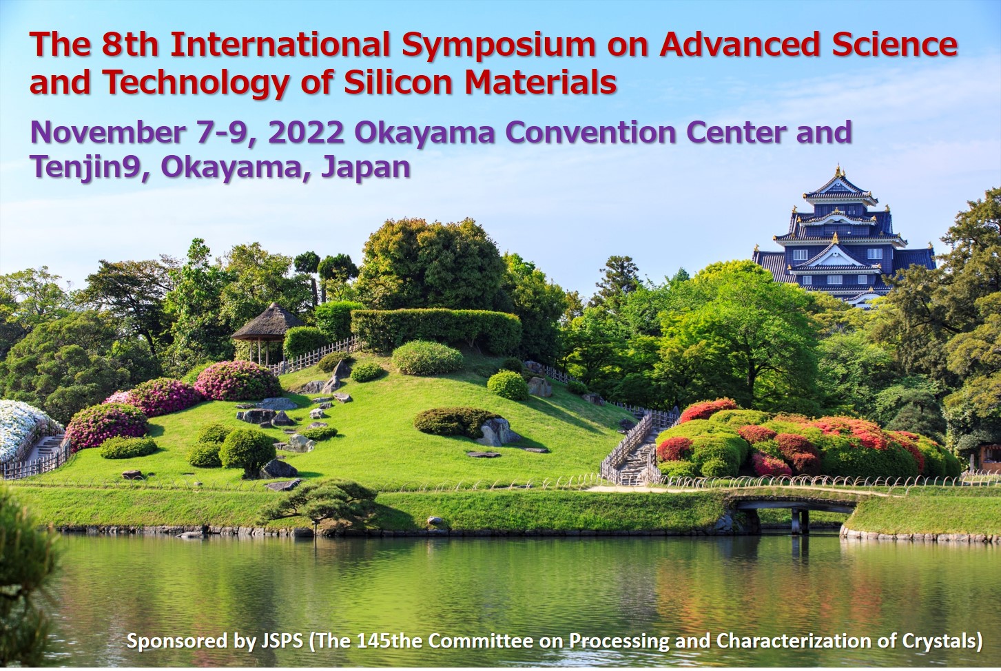
will hold The Eighth International Symposium on Advanced Science and Technology of Silicon at Okayama Convention Center and Tenjin9, Okayama, Japan,
on November 7-9, 2022. The first, second, third, fourth, fifth, sixth and seventh symposia were held at the same location in November of 1991, 1996,
2000, 2004, 2008, 2012, and 2016 respectively. The Symposium provides a valuable opportunity for scientists and engineers engaged in fundamental and
applied research on silicon and related materials to discuss basic problems and new possibilities in this field. The Symposium will cover broad aspects
of physics and recent technologies using silicon related materials and devices. The program will be arranged to provide ample time for discussion and
communication among participants. Accordingly, the number of oral presentations consisting mainly of invited talks will be limited. Contributions to the
program in the form of poster presentation will be welcome. Given the nature of Symposium, the number of attendees will be limited to approximately 100.
Further information can be obtained from the Symposium homepage (http://gakushin145.kir.jp/hawaii2020).
Topics
Crystal growth and wafer technology
- Point-defect controlled wafer, Epi wafer, Annealed wafer
- SOI, GOI, Strained Si wafer
- Advanced wafer processing
Advanced characterization technology
- Electron microscopy
- X-ray diffraction
- FTIR, PL, Other spectroscopic and optical imaging techniques
Defects and impurities
- Point defects, Diffusion, Gettering
- Strain and stress
- Defect engineering for emerging materials
Photovoltaic Si
- Impurities and defects in solar cell materials
- Crystal growth and advanced processing
Group IV semiconductor-based device technology
- New materials for advanced CMOS devices
- Si power devices
SiC, Nitride semiconductors and other wide-bandgap materials
- Bulk and epitaxial growth, Processing
- Defect characterization
- Power, high-frequency, and optical devices including LED and LD
Materials Informatics
